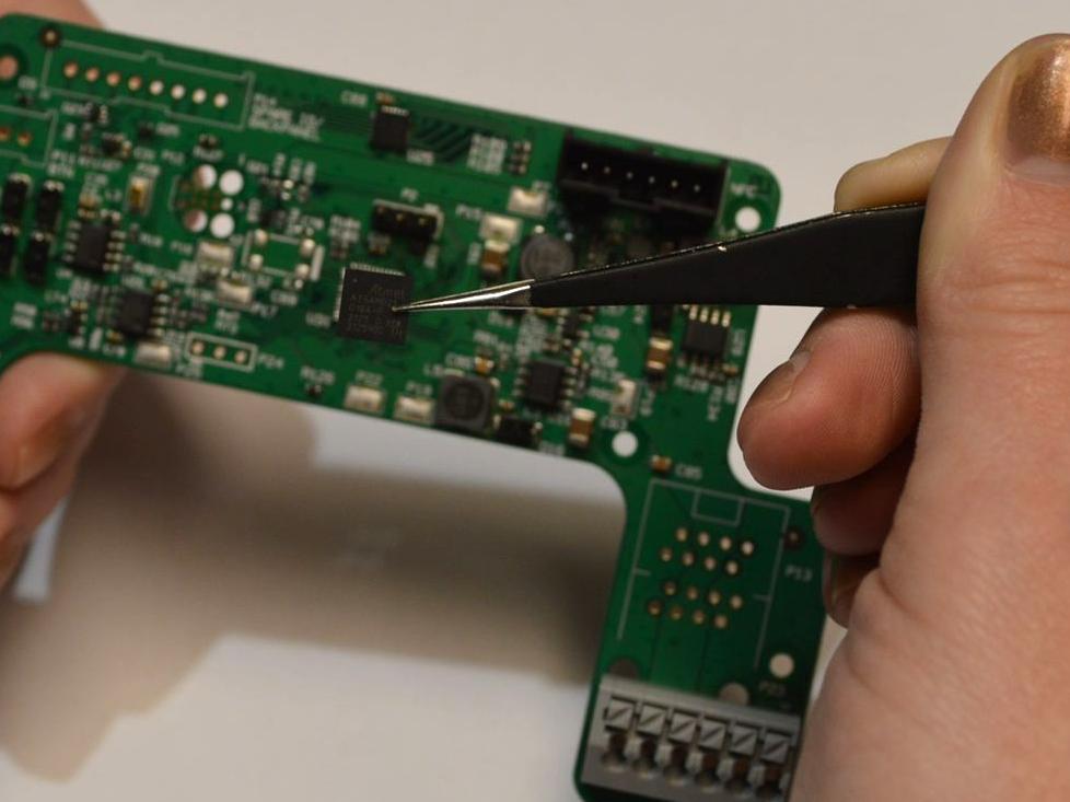
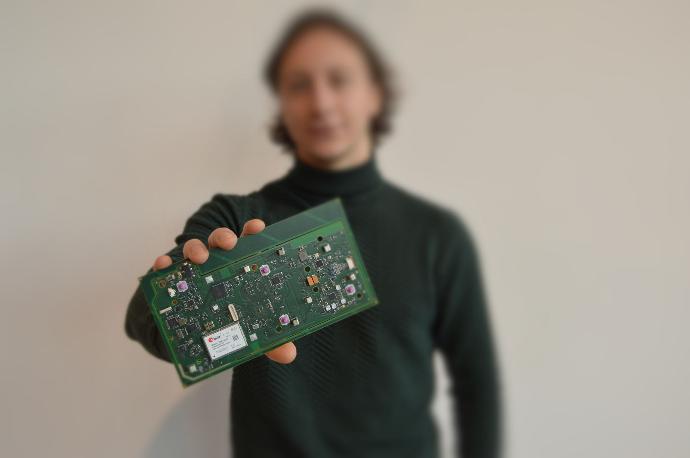
A hardware designer is responsible for the development of the electronic part of your product: they design the printed circuit board(s) (PCB), by the accompanying schematics and layouts. By first drawing a schematic, they can eventually draw the PCB. In cooperation with the software designers, they ensure that the design of the system architect is realised, so that the result works as desired by the customer. These PCBs, once assembled with the right components, are the element on which the software is installed and which turns our customer's idea into a working product. The mechanical requirements and workings are taken into account so that all the hardware and mechanical elements fit together flawlessly - especially if this element is also carried out in-house by the VEDS Group.
we specialise in
PCB design
from single to multi-layer PCB
flex & flex-rigid PCB
high speed & RF signal lay-outs
high density interconnects (HDI)
differential pairs
BGA & FPGA design
controlled impendance
integration of sensors & matched lenght
analog tot digital design
bussystems
RISC based-solutions
module-integrations (x86, RISC, m2.com)
blind, buried & micro via's

PCB design: schematics
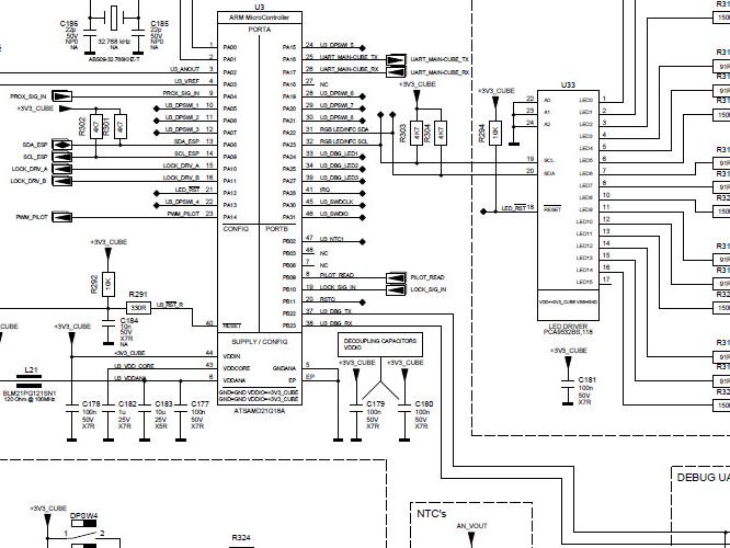
After consultation with the customer regarding the wishes and details of the product to be developed, PCB design is the start of the project. This part consists of two different steps: making the schematic diagram and drawing the layout. First, the engineer begins by drawing a schematic. This can be seen as a kind of blueprint for the placement and layout of components and electrical connections (via's). A correct schematic is a well-structured circuit diagram that clearly shows the vias between the various components, which lays the foundation for the layout. de lay-out.

PCB design: lay-out
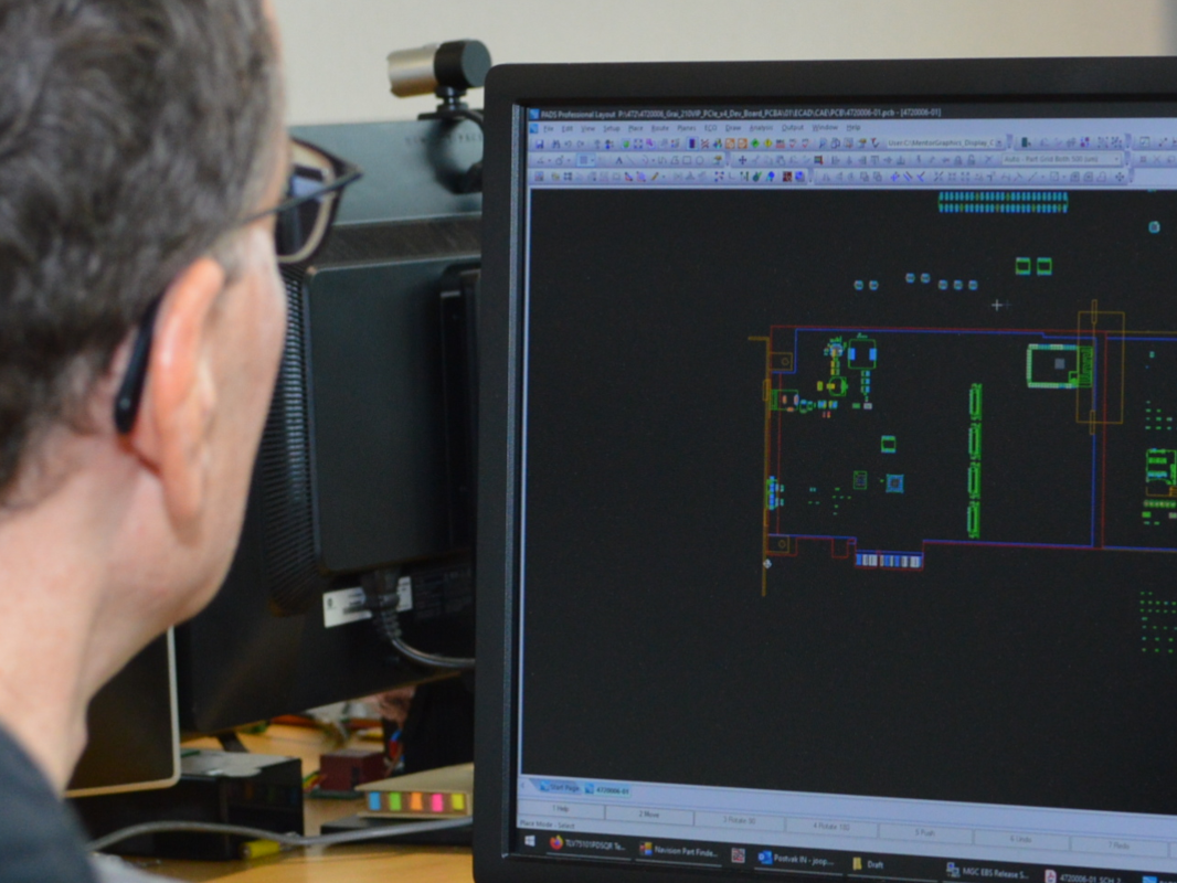
After the schematic has been completed, the engineer picks up the layout. Here, the engineer places the parts - the components and electronic connections (via's) - in the right place on the PCB. Sometimes this requires several variants of placement to achieve the desired final result. This takes into account the PCB size, the number of layers and any specifications relating to mechanical requirements. The advantage of having all the designs drawn in-house is that all the designs are perfectly attuned to each other.
VEDS Group has the following hardware design packages at its disposal:
Mentor Graphics PADS
Allegro
Altium

component choice
During the design phase of the PCB, our hardware engineers decide which components are to be placed at which locations on the PCB. Due to both the rapid development of components and the current hectic market for components, it has recently become increasingly common for components to be unavailable or have limited availability. This can lead to enormous delays in the delivery time of a product, so that our partners and customers cannot deliver their products. In these cases, our hardware engineers ensure that suitable alternatives are considered where possible.
read more about our other departments and get to know us better
software
An (embedded) software designer designs, improves and maintains software written for electronic devices and machines, (computer) programmes and applications based on the requirements and wishes of the customer. The (embedded) software designer carries out extensive tests and checks during the development of the new software before it is used by the final users.
mechanics
A mechanical designer designs technical illustrations for electronic devices and machines and takes care of the production of prototypes (and series). The designs are made according to the wishes of the customer and in consultation with the hardware and software engineers for the best result. Mechanical designers ensure that the designs are functional, efficient and safe.
production & assembly
The production and assembly staff ensure that the designed products come to life. The production department produces and assembles the PCBs using a stencil-, SMD- and soldering machine and provides conventional hand assembly and (final) checks. The assembly department ensures that the end products are assembled according to the customer's wishes.
completed projects
We carry out our projects for and with our clients, with whom the VEDS Group wishes to create a liveable, technological world together. Are you curious about concrete examples of completed projects and products? We have listed a number of them for you.
do you have any questions about our services or products?
ask for the possibilities.
contact details
VEDS Group
high tech campus 25, hal 2
5656AE Eindhoven
Netherlands
phone: +31 (0)88 011 02 02
mail: info@veds.nl
